当前课程知识点:数字逻辑电路 > Chapter8 Generation and Shaping of Pulse Signal > Test8 > Chapter4 Boolean Algebra and Logic Simplification
Chapter4 Boolean Algebra and Logic Simplification
本章导读
1854年,乔治·布尔发表了《思维规律研究》。该系统的的基础是二元方法,仅处理二个对象。是-否、真-假、开-关、0-1等。建立了逻辑学和数学理论概率。布尔代数是一种方便的代数系统的表达和分析方法逻辑电路的操作。本章将学习如何使用布尔代数和卡诺图简化逻辑电路。布尔代数的运算律(operational rule of Boolean algebra)是布尔代数的基本运算法则,布尔代数中的变量代表一种状态或概念,数值1或0并不是表示变量在数值上的差别而是代表状态与概念存在与否的符号。布尔代数主要运算法则有:结合律,交换律,分配律,吸收律,幂等律等。
逻辑函数的化简
从以上逻辑代数基本定律的介绍中(特别是分配律、吸收律和反演律)不难发现,等式两边的表达式虽然不同,但却是等价的,逻辑功能是相同的。也就是说,同一函数可以有不同的表达形式,每一表达式都可画出与其相应的逻辑图。逻辑表达式最简单的标准有两个:一是所含乘积项的个数最少;二是在前一条件下,每个乘积项中变量的个数也最少。常用的化简方法有两种:代数法和卡诺图法。
(1)代数法
代数法(又叫公式法)化简是利用布尔代数的基本运算法则和基本定律对较复杂的逻辑函数式进行演算化简的方法。如何使逻辑函数式达到最简,在很大程度上依赖人们对逻辑运算掌握的熟练程度和实践经验。下面介绍几种常用的化简方法 。
①并项法
利用互补律:A+A'=1,并项后消去变量。
例 化简ABC+A'BC
解 Y=(A+A')BC=BC
②吸收法
利用吸收律:A+AB=A,吸收多余项,消去多余变量。
例 化简Y=AB+ABC
解 Y=(AB)+(AB)C=AB
或 Y=AB(1+C)=AB ·
③消去法
利用吸收律、分配律、摩根定律等消去多余因子。
例 化简Y=AB+A'C+B'C
解 Y=AB+(A'+B')C=AB+(AB)'C=(AB)+(AB)'C=AB+C
④配项法
利用A+A'=1,A+1=1等,先把一项拆成两项,再重新与其他项组合进行化简,消去更多的项。
例 化简Y=AB+BC+(AC)'
解 Y=AB(C+C')+BC+AC'=ABC+ABC'+BC+AC'
=(A+1)BC十AC'(B+1)=BC+AC'
代数法化简没有一个固定的模式,往往要综合运用多种方法。多加练习,熟能生巧,逐步积累经验才能运用自如。
(2)卡诺图法
卡诺图化简法是1953年由卡诺首先提出来用于化简逻辑函数,它是逻辑函数的最小项按相邻关系排列的方格图。
本章要点
4–1 Boolean Operations and Expressions
4–2 Laws and Rules of Boolean Algebra
4–3 DeMorgan’s Theorems
4–4 Boolean Analysis of Logic Circuits
4–5 Logic Simplification Using Boolean Algebra
4–6 Standard Forms of Boolean Expressions
4–7 Boolean Expressions and Truth Tables
4–8 The Karnaugh Map
4–9 Karnaugh Map SOP Minimization
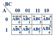
图1 三变量卡诺图
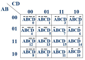
图2 四变量卡诺图
-1.1 Structure and Methods
-1.2 Introductory
-Chapter1 Introductory Concepts
-Test1
-2.1 Number Systems
-2.2 Codes
-Chapter2 Number systems and Codes
-Test2
-3.1 Logic Gates(1)
-3.2 Logic Gates(2)
-Test3
-4.1 Boolean Algebra
-4.2 Logic Simplification
-Chapter4 Boolean Algebra and Logic Simplification
-Test4
-5.1 Analysis of combination logic circuit
--5-1 Analysis of combination logic circuit
-5.2 Design of combination logic circuit
--5-2 Design of combination logic circuit
-5.3 Half and Full Adders
-5.4 Encoders
-5.5.1 Decoders(1)
-5.5.2 Decoders(2)
-5.5.3 Decoders(3)
-5.5.4 Decoders(4)
-5.6.1 Multiplexers (Data Selectors)(1)
--5-6 Multiplexers (Data Selectors)(1)
-5.6.2 Multiplexers (Data Selectors)(2)
--5-6 Multiplexers (Data Selectors)(2)
-5.7 Comparators
-Chapter5 Combinational Logic Circuit
-Test5
-6.1 Latches
-6.2 Flip-Flops
-6.3 Flip-Flops Applications
-Test6
-7.1 Analysis of Sequential logic circuit-1
--7–1 Analysis of Sequential logic circuit-1
-7.2 Analysis of Sequential logic circuit-2
--7–2 Analysis of Sequential logic circuit-2
-7.3 Design of Sequential logic circuit-1
--7.3 Design of Sequential logic circuit-1
-7.4 Design of Sequential logic circuit-2
--7-4 Design of Sequential logic circuit-2
-7.5 Counters-1
-7.6 Counters-2
-7.7 Registers-1
-7.8 Registers-2
-Chapter7 Sequential Logic Circuit
-Test7
-8.1 555 Timer circuit structure and working principle
--8.1 555 Timer circuit structure and working principle
-8.2 Application circuit of 555 Timer
--8.2 Application circuit of 555 Timer
-Chapter8 Generation and Shaping of Pulse Signal
-Test8