
当前课程知识点:数字逻辑电路 > Chapter8 Generation and Shaping of Pulse Signal > Test8 > Chapter6 Flip-Flops
Chapter6 Flip-Flops
本章导读
在实际的数字系统中包含大量的存储单元,而且经常要求他们在同一时刻同步动作,为达到这个目的,在每个存储单元电路上引入一个时钟脉冲(CLK)作为控制信号,只有当CLK到来时电路才被“触发”而动作,并根据输入信号改变输出状态。把这种在时钟信号触发时才能动作的存储单元电路称为触发器,最常见的是D触发器和JK触发器,其中D触发器构成芯片是74LS74,CP脉冲上升沿触发有效,而JK触发器构成芯片是74LS112,CP脉冲下升沿触发有效。
Flip-flops are synchronous bistable devices, also known as bistable multivibrators. In this case, the term synchronous means that the output changes state only at a specified point (leading or trailing edge) on the triggering input called the clock (CLK), which is designated as a control input, C; that is, changes in the output occur in synchronization with the clock. Flip-flops are edge-triggered or edge-sensitive whereas gated latches are level-sensitive.
The D input of the D flip-flop is a synchronous input because data on the input are transferred to the flip-flop’s output only on the triggering edge of the clock pulse. When D is HIGH, the Q output goes HIGH on the triggering edge of the clock pulse, and the flip-flop is SET. When D is LOW, the Q output goes LOW on the triggering edge of the clock pulse,and the flip-flop is RESET.
The J and K inputs of the J-K flip-flop are synchronous inputs because data on these inputs are transferred to the flip-flop’s output only on the triggering edge of the clock pulse. When J is HIGH and K is LOW, the Q output goes HIGH on the triggering edge of the clock pulse, and the flip-flop is SET. When J is LOW and K is HIGH, the Q output goes LOW on the triggering edge of the clock pulse, and the flip-flop is RESET. When both J and K are LOW, the output does not change from its prior state. When J and K are both HIGH, the flip-flop changes state. This called the toggle mode.
本章要点
6–1 Flip-Flops
6–2 Flip-Flop Operating Characteristics
6–3 Flip-Flop Applications
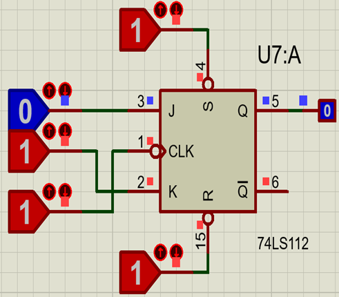
图1 JK触发器的仿真电路
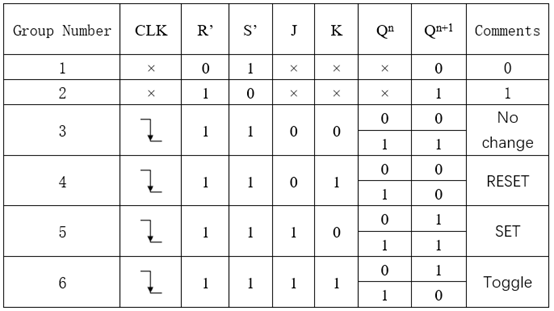
图2 JK触发器的功能真值表
-1.1 Structure and Methods
-1.2 Introductory
-Chapter1 Introductory Concepts
-Test1
-2.1 Number Systems
-2.2 Codes
-Chapter2 Number systems and Codes
-Test2
-3.1 Logic Gates(1)
-3.2 Logic Gates(2)
-Test3
-4.1 Boolean Algebra
-4.2 Logic Simplification
-Chapter4 Boolean Algebra and Logic Simplification
-Test4
-5.1 Analysis of combination logic circuit
--5-1 Analysis of combination logic circuit
-5.2 Design of combination logic circuit
--5-2 Design of combination logic circuit
-5.3 Half and Full Adders
-5.4 Encoders
-5.5.1 Decoders(1)
-5.5.2 Decoders(2)
-5.5.3 Decoders(3)
-5.5.4 Decoders(4)
-5.6.1 Multiplexers (Data Selectors)(1)
--5-6 Multiplexers (Data Selectors)(1)
-5.6.2 Multiplexers (Data Selectors)(2)
--5-6 Multiplexers (Data Selectors)(2)
-5.7 Comparators
-Chapter5 Combinational Logic Circuit
-Test5
-6.1 Latches
-6.2 Flip-Flops
-6.3 Flip-Flops Applications
-Test6
-7.1 Analysis of Sequential logic circuit-1
--7–1 Analysis of Sequential logic circuit-1
-7.2 Analysis of Sequential logic circuit-2
--7–2 Analysis of Sequential logic circuit-2
-7.3 Design of Sequential logic circuit-1
--7.3 Design of Sequential logic circuit-1
-7.4 Design of Sequential logic circuit-2
--7-4 Design of Sequential logic circuit-2
-7.5 Counters-1
-7.6 Counters-2
-7.7 Registers-1
-7.8 Registers-2
-Chapter7 Sequential Logic Circuit
-Test7
-8.1 555 Timer circuit structure and working principle
--8.1 555 Timer circuit structure and working principle
-8.2 Application circuit of 555 Timer
--8.2 Application circuit of 555 Timer
-Chapter8 Generation and Shaping of Pulse Signal
-Test8